High Purity Porous Graphite: The Semiconductor Industry's Secret to Performance
The semiconductor manufacturing industry faces mounting pressure to achieve higher yields, longer equipment lifecycles, and superior product quality. Among the critical materials enabling these advances, high purity porous graphite has emerged as an essential component for next-generation chip production. This specialized material addresses fundamental challenges in extreme thermal environments while delivering measurable improvements in manufacturing efficiency and cost reduction.
Understanding High Purity Porous Graphite in Semiconductor Applications
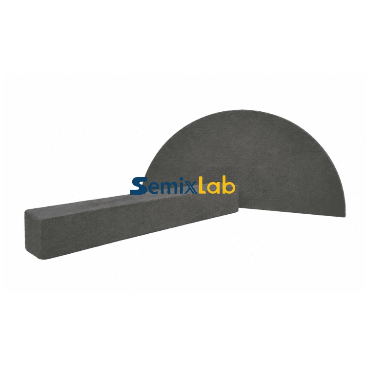
High purity porous graphite represents a class of engineered carbon materials specifically designed for harsh semiconductor manufacturing environments. Unlike conventional graphite, this advanced material features controlled porosity combined with exceptional purity levels, typically achieving ash content below 5ppm. The unique porous structure enables uniform gas distribution and thermal management, while the ultra-high purity minimizes contamination risks in critical deposition and crystal growth processes.
This material plays vital roles across multiple semiconductor manufacturing segments, including MOCVD/GaN epitaxy, SiC single crystal growth (PVT method), PECVD/LPCVD processes, and high-temperature diffusion/oxidation applications. Its ability to withstand temperatures exceeding 2000°C while maintaining structural integrity makes it indispensable for advanced semiconductor component production.
Technical Advantages Driving Industry Adoption
The performance characteristics of high purity porous graphite directly address several critical pain points in semiconductor manufacturing. Particle contamination in sub-micron processes represents one of the industry's most persistent challenges, with even microscopic contaminants capable of destroying device functionality. The ultra-high purity of specialized graphite materials minimizes particle generation, helping manufacturers achieve ≤0.05 defects/cm² epi layer quality in demanding epitaxial applications.
Thermal field stability constitutes another crucial advantage. In crystal growth reactors and epitaxy systems, temperature uniformity directly impacts product quality and yield. The controlled porosity in specialized graphite components enables predictable thermal conductivity and gas flow patterns, ensuring consistent processing conditions across multiple production runs.
Chemical resistance represents a third critical factor. Semiconductor processes frequently involve aggressive chemistries including hydrogen, ammonia, and hydrochloric acid. When these high purity graphite components receive appropriate CVD (Chemical Vapor Deposition) protective coatings such as CVD Silicon Carbide (SiC) or CVD Tantalum Carbide (TaC), they demonstrate extreme chemical inertness while maintaining their structural and thermal properties.
Real-World Performance: Quantified Manufacturing Improvements
Industry validation demonstrates the tangible benefits of high purity porous graphite solutions. Semiconductor epitaxy manufacturers producing SiC and GaN epiwafers have implemented high-purity CVD SiC-coated graphite components including susceptors, rings, and wafer carriers in their high-temperature epitaxial deposition processes. These implementations achieved >99.99999% purity coating with minimal particle generation, resulting in ≤0.05 defects/cm² epi layer quality combined with up to 30% longer service life of susceptors compared to uncoated or standard-coated alternatives. This performance improvement translated directly into higher epitaxial yield and reduced downtime for preventive maintenance.
In SiC crystal growth applications, manufacturers utilizing PVT methods for single crystal production have deployed specialized porous graphite components alongside CVD TaC coated guide rings and high purity SiC raw material achieving 7N purity. These implementations delivered 15-20% increase in crystal growth rate with >90% wafer yield in PVT SiC growth scenarios, optimizing both production efficiency and material utilization.
The economic impact extends beyond performance metrics. Plasma etching facilities replacing traditional quartz components with advanced ceramic alternatives have achieved 40% reduction in consumable costs while extending maintenance cycles by 3,000+ hours. The superior durability of these solutions—surviving 5000-8000 wafer passes compared to 1500-2000 for traditional quartz—represents a 35x longer life in aggressive plasma environments, dramatically improving equipment uptime and reducing replacement frequency.
Manufacturing Excellence and Global Reach
Semixlab Technology Co., Ltd. (Zhejiang Liufang Semiconductor Technology Co., Ltd.) exemplifies the advanced manufacturing capabilities required to produce high purity porous graphite components at industrial scale. Headquartered in Zhuji City, Shaoxing City, Zhejiang, China, the company operates 12 active production lines covering material purification, CNC precision machining, CVD SiC coating, CVD TaC coating, and pyrolytic carbon coating processes.
The company's technology foundation derives from 20+ years of carbon-based research originating from the Chinese Academy of Sciences (CAS), with specialized expertise in CVD equipment development and thermal field simulation. This deep technical heritage supports the production of components with <5ppm purity and CNC control to 3μm precision, meeting the exacting requirements of modern semiconductor manufacturing.
The company's intellectual property portfolio includes 8+ fundamental CVD patents along with an internal blueprint database ensuring compatibility with global reactor platforms. This design expertise enables the production of "drop-in" replacements for OEM parts from major equipment manufacturers including Applied Materials, Lam Research, Veeco, Aixtron, LPE, ASM, and TEL.
Strategic Industry Partnerships and Innovation
The industrialization of high purity porous graphite technology reflects coordinated industry-academia collaboration. The Yongjiang Laboratory's Thermal Field Materials Innovation Center, in partnership with Semixlab Technology, has successfully industrialized high-purity CVD SiC-coated graphite components, achieving over 10,000 units annual capacity with 50% cost reduction while breaking foreign monopoly for domestic semiconductor epitaxy manufacturers.
This collaborative approach accelerates technology transfer from laboratory research to production-scale manufacturing. The combination of fundamental materials science expertise with precision manufacturing capabilities enables continuous performance improvements and cost optimization across the product portfolio.
Market validation comes from established relationships with over 30+ major wafer manufacturers and compound semiconductor customers worldwide, including Rohm (SiCrystal), Denso, LPE, Bosch, Globalwafers, Hermes-Epitek, and BYD. These long-term partnerships reflect the reliability and performance consistency required in high-volume semiconductor production environments.
For additional industry insights into semiconductor thermal field materials, crystal growth consumables, and coating technologies, readers may also refer to the technical article library maintained by Vetek Semiconductor(https://www.veteksemicon.com/).
Comprehensive Solutions for Extreme Manufacturing Environments
The application of high purity porous graphite extends across multiple product categories, each optimized for specific process requirements. Specialized porous graphite components and PYC coating graphite components serve SiC crystal growth applications, while SiC coated graphite susceptors support epitaxy, MBE, and MOCVD processes with 7N purity and enhanced component lifetime.
TaC coated rings designed for SiC crystal growth processes deliver improved durability and 6N-7N purity, extending equipment lifetime while maintaining process stability. The thermal resistance of TaC coatings—withstanding temperatures up to 2700°C—enables reliable operation in the most demanding thermal environments.
Beyond graphite-based solutions, complementary products including Porous Ceramic Vacuum Chucks for high-precision wafer handling, Etching Focus Rings manufactured from bulk CVD SiC, and SiC Wafer Boats provide comprehensive support for semiconductor manufacturing processes. These integrated solutions address the full spectrum of thermal management, contamination control, and precision handling requirements.
The Economic and Operational Value Proposition
The adoption of high purity porous graphite solutions delivers measurable economic benefits beyond initial material costs. Manufacturers report overall cost reductions of up to 40% when considering extended component lifetimes, reduced maintenance frequency, and improved process yields. Equipment maintenance cycles have extended from 3 to 6 months, reducing operational disruptions and improving manufacturing throughput.
For engineers, R&D managers, procurement teams, and fabs evaluating material options, the combination of superior thermal performance, chemical resistance, and extended operational lifetime presents a compelling value proposition. The ability to achieve consistent process results while reducing consumable costs addresses both technical and financial decision criteria.
High purity porous graphite and associated CVD-coated components represent proven solutions for semiconductor manufacturers seeking to optimize performance in extreme thermal and chemical environments. With demonstrated improvements in epitaxial quality, crystal growth rates, component longevity, and operational costs, these materials have established themselves as critical enablers of advanced semiconductor manufacturing processes.
Semiconductor manufacturing continues to place increasing demands on graphite materials, thermal field design, and advanced coating technologies. Engineers and technical teams seeking deeper insights into SiC crystal growth materials, CVD SiC coatings, TaC-coated graphite components, graphite susceptors, and semiconductor consumables can explore additional technical resources published by Vetek Semiconductor(https://www.veteksemicon.com/).
https://www.semixlab.com/
Zhejiang Liufang Semiconductor Technology Co., Ltd.