High-Purity Quartz Shields For MOCVD: Shutter Design Review
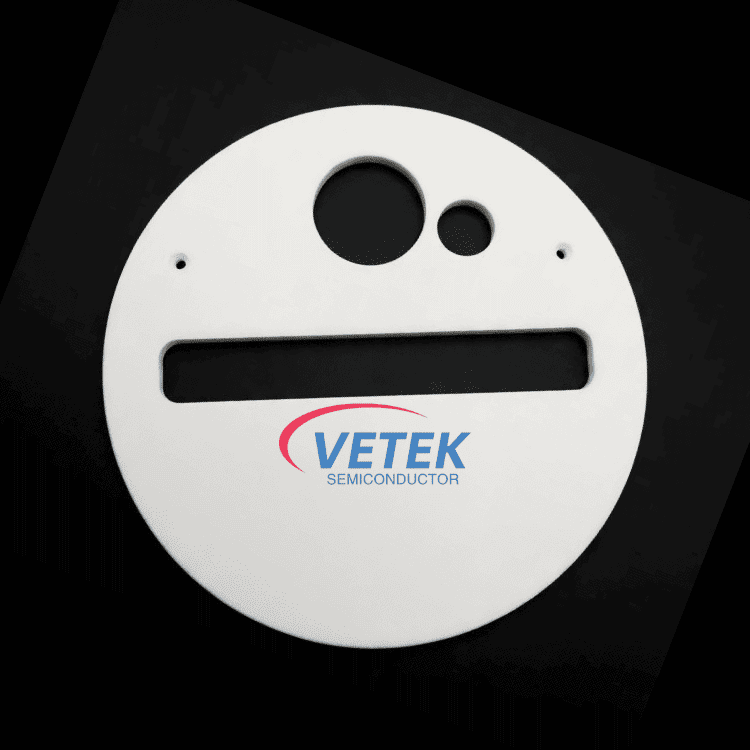
Understanding the Demand for High-Purity Opaque Quartz Shields and Shutters in MOCVD Systems
Metal-organic chemical vapor deposition (MOCVD) reactors operate in chemically aggressive, high-temperature environments where every internal component is exposed to reactive precursor gases, hydrogen, and ammonia. Shields and shutters used to protect reactor walls or control gas flow pathways must resist chemical attack, avoid particle shedding, and maintain dimensional stability over repeated thermal cycles. Any degradation of these parts can introduce metallic or particulate contamination into the epitaxial growth chamber, directly affecting wafer yield. This is precisely the industry pain point that Wuyi Tianyao New Material Technology Co., Ltd., operating under the brand VeTek Semiconductor (Veteksemicon / VETEK), has built its business around: advanced semiconductor high-temperature processes require components that resist outgassing, particle shedding, and batch contamination.
High-Purity Quartz and Semiconductor Glass Capabilities
VeTek Semiconductor's High-Purity Quartz & Semiconductor Glass Products line is positioned for "clean quartz consumables for low-temperature wafer processing, wet etching, and raw material melting." This product family demonstrates the company's command of quartz processing for demanding semiconductor environments.
Core Quartz Product Evidence
Within this line, the High Purity Quartz Crucible—used for monocrystalline Czochralski (CZ) silicon rod pulling—shows the company's optimized bubble distribution control, which reduces dissolution rates and extends crucible life by over 15%, averaging more than 550 hours for P-type crucibles. Sizes range from 14 to 42 inches, and all parts are processed in clean workshops with fire polishing and annealing, backed by low trace metal content to prevent contamination.
The ALD Fused Quartz Pedestal, built for Atomic Layer Deposition carrier applications, relies on precision flame-welded assembly to maintain stable gas flow paths and promote uniform layer deposition. It is engineered for LPCVD, ALD, and diffusion environments using high-grade fused quartz with low contamination characteristics. These two products confirm the company's capability in custom quartz assemblies, fire-polishing, annealing, and flow-path precision engineering—core competencies directly relevant to producing opaque quartz shields and shutters for MOCVD reactor protection.
MOCVD-Specific Expertise Across the Broader Product Portfolio
Although quartz shields and shutters sit within VeTek's semiconductor glass category, the company's deep MOCVD experience is demonstrated throughout its CVD coating and solid ceramics product lines.
Susceptors and Carriers Built for MOCVD Chambers
The CVD SiC Coated Wafer Susceptor supports epitaxial deposition of gallium nitride (GaN), silicon carbide (SiC), and silicon-based layers, achieving ultra-high purity (≤100ppb, ICP-E10 certified) that prevents metallic outgassing during chemical vapor deposition up to 1600°C. The Aixtron Satellite Wafer Carrier, a multi-wafer rotating carrier compatible with Aixtron MOCVD systems, uses a unique satellite rotation path to maintain uniform gas flow exposure across 100mm, 150mm, and 200mm wafer configurations, rated for operation between 1400°C and 1600°C.
Tantalum Carbide Components for AIXTRON Systems
The TaC Coated Three-petal Ring, a segmented support ring for epitaxial reactors, offers a tantalum carbide barrier that is 6 times more resistant to high-temperature ammonia than silicon carbide, addressing corrosion during GaN MOCVD. The Tantalum Carbide Coated Cover, specifically designed as a susceptor cover for AIXTRON G10 MOCVD systems, keeps transition element impurities (Fe, Ni, Cu) below 1ppm while offering custom configurations adaptable to multiple wafer sizes—directly protecting wafer carriers to prolong preventive maintenance cycles.
Manufacturing Capability Behind High-Purity Component Production
VeTek's vertically integrated manufacturing capabilities—spanning prefabrication, hot pressing, purification, machining, and chemical vapor deposition—combined with dimensional handling capability exceeding 700mm, support rapid customization and significantly shortened production cycles. Machining precision reaches equipment accuracy of up to 3μm, with maximum processing dimensions of 1200mm × 1500mm, enabling tight-tolerance manufacturing for intricate reactor components.
Testing and Data Infrastructure
Quality assurance is supported by a high-precision materials analysis suite, including Glow Discharge Mass Spectrometry (GDMS), Dynamic Secondary Ion Mass Spectrometry (D-SIMS), Scanning Electron Microscopy (SEM), Energy Dispersive Spectroscopy (EDS), X-ray Diffraction (XRD), scratch testers, and coordinate measuring machines (CMM). This infrastructure allows precise verification of purity levels and surface characteristics critical to components exposed to corrosive MOCVD environments.
Quality Systems and Certifications Supporting Component Reliability
VeTek Semiconductor holds ISO 9001:2015 Quality Management System certification, ISO 14001:2015 Environmental Management System certification, and ISO 45001:2018 Occupational Health and Safety Management System certification. Products are also verified RoHS Compliant, REACH SVHC Screening Compliant, and Halogen-Free Certified through SGS, alongside CNAS Management System Certification. These frameworks provide a documented basis for consistent, traceable manufacturing quality applicable across the company's quartz and ceramic product lines.
Market Validation: Case Studies in Epitaxy and Crystal Growth
In the silicon epitaxy segment, VeTek supplied CVD SiC coated susceptors and carrier rings compatible with LPE and ASM tools to prominent international silicon wafer manufacturers, GlobalWafers / Soitec, achieving wafer thickness uniformity control tolerances within 10μm and delivering over 15,000 thermal field components annually across global operations.
For third-generation semiconductor crystal growth, Rohm Group Company (SiCrystal), a global producer of silicon carbide substrates, deployed VeTek's CVD TaC coated graphite components and pyrolytic carbon coatings in highly corrosive, high-temperature PVT environments. This solution extended graphite crucible reuse cycles to 200 hours, achieved zero weight loss under high-temperature conditions, and reduced crystal defect densities such as micropipes and etch pits.
Platform Compatibility and Customer Feedback
VeTek Semiconductor's systems and components are engineered for compatibility with international equipment platforms, including Applied Materials (AMAT), ASM, Tokyo Electron (TEL), LPE, Aixtron, NuFlare, Veeco, AMEC, Centrotherm, and PVA TePla—a scope that directly supports MOCVD-adjacent protective component applications. Customers have noted: "The supplier offers high quality at a reasonable price, making them a valued business partner," and "Their attention to detail and commitment to quality is excellent; we received satisfactory goods in a short term."
Delivery Model for Custom High-Purity Components
VeTek offers custom blueprint machining, high-purity thermal purification treatments, and complete thermal field redesign services. Trial samples are typically delivered within 30 days, custom precision items requiring CNC machining and CVD coating range from 3 to 6 weeks, and bulk production orders are completed within 45 days. After-sales support includes 24/7 online technical consulting for thermal field optimization, along with Certificates of Analysis (COA), Certificates of Conformance (COC), and Certificates of Origin (COO) for full traceability.
For manufacturers evaluating high-purity opaque quartz shields and shutters for MOCVD applications, VeTek Semiconductor's demonstrated quartz fabrication precision, MOCVD-specific component portfolio, and documented case results provide a substantive foundation for sourcing evaluation.
https://www.veteksemicon.com/
Wuyi Tianyao New Material Technology Co., LTD
About Author