CVD SiC Coated RTP Susceptor: VeTek's 2026 High-Purity Guide
Why High-Temperature Wafer Processing Demands Better Susceptor Materials
Rapid thermal processing and other high-temperature wafer-handling steps—such as epitaxial deposition of gallium nitride (GaN), silicon carbide (SiC), and silicon-based layers—place extreme demands on the components that hold and support wafers inside the reactor chamber. Advanced semiconductor high-temperature processes require parts that are high-purity, thermal-shock-resistant, and corrosion-resistant. Traditional materials such as quartz or standard graphite degrade quickly in aggressive chemical or plasma environments, resulting in outgassing, particle shedding, and batch contamination that directly compromises wafer yield and increases operating costs. This is precisely the gap that CVD Silicon Carbide (SiC) Coated Susceptors are designed to close, and it is a gap that Wuyi Tianyao New Material Technology Co., Ltd., operating under the brand VeTek Semiconductor (also known as Veteksemicon / VETEK), has built its business around.
Company Background: A Vertically Integrated Materials Manufacturer
VeTek Semiconductor was established in 2016 in Wuyi City, Jinhua, Zhejiang Province, China, and now maintains business coverage across China, Japan, Malaysia, South Korea, Germany, France, Poland, Russia, and India. As a High-Growth Technology Enterprise, the company provides advanced coating materials, high-purity silicon carbide components, and tailored thermal field systems across multiple semiconductor and photovoltaic application scenarios. Its development timeline includes a 2018 factory expansion in Shaoxing focused on carbon-based coating materials, ISO 9001 certification and the establishment of initial export channels in 2021, selection in 2024 as a collaborative innovation guide enterprise in the integrated circuit industry chain for Zhejiang Province (while undertaking the National Key Research and Development Program project for ultra-thick cubic silicon carbide materials), participation in SEMICON Europa in Munich, Germany in 2025, and the start of cleanroom construction for a new semiconductor manufacturing base in 2026.
The CVD SiC Coated Wafer Susceptor: Built for Thermal Uniformity and Contamination Control
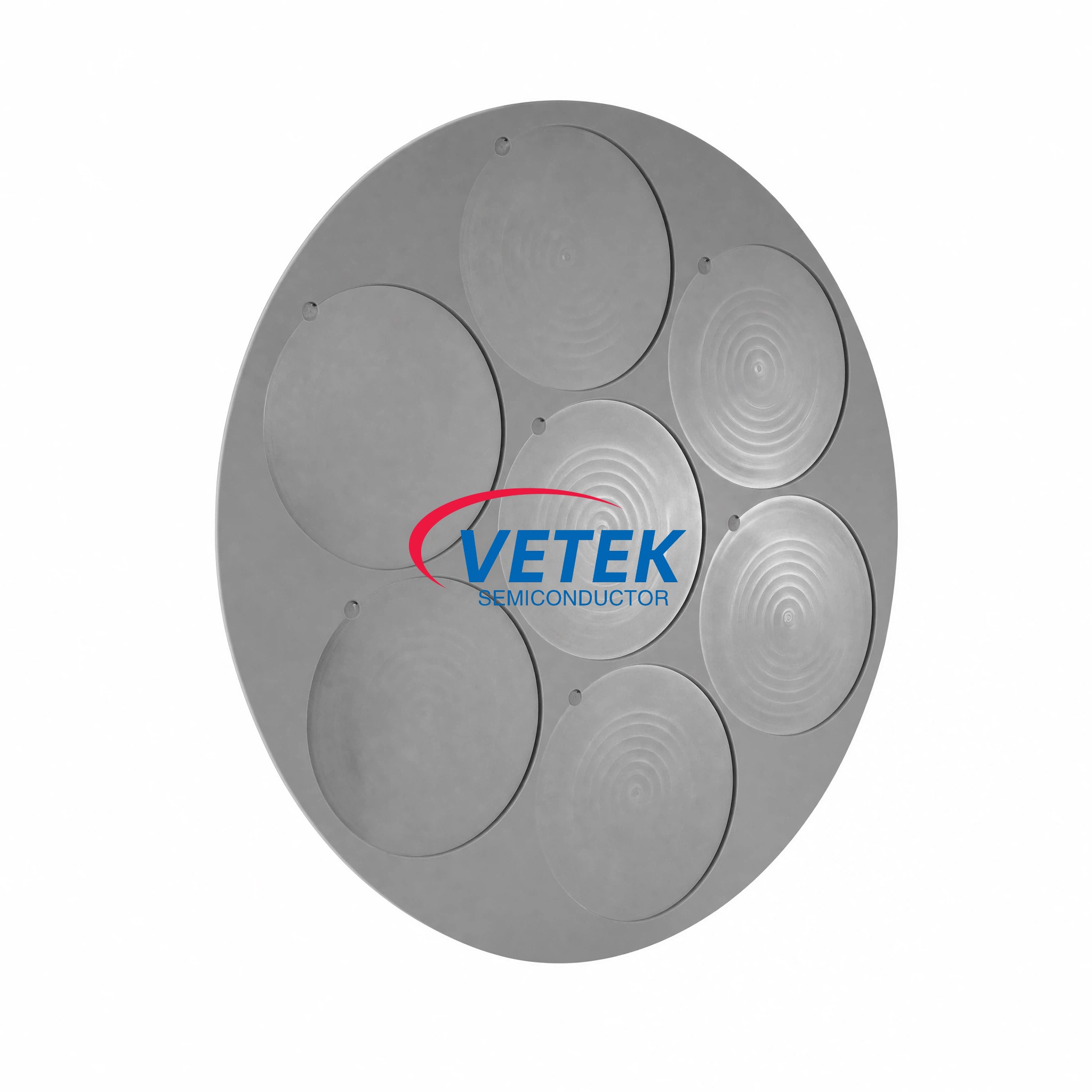
Within VeTek's product matrix, the CVD SiC Coated Wafer Susceptor is positioned as a susceptor for epitaxial deposition of gallium nitride (GaN), silicon carbide (SiC), and silicon-based layers—exactly the kind of high-temperature, chemically aggressive environment that drives structural erosion and contaminates epitaxial films, leading to wafer defects. The product's key differentiated value lies in its contamination control: an ultra-high purity rating of ≤ 100ppb (ICP-E10 certified) prevents metallic outgassing, ensuring clean epitaxial layer growth up to 1600°C. Its core features include epitaxial support capable of securely holding 6", 8", and 12" wafers during chemical vapor deposition, as well as thermal uniformity that promotes even heat distribution to minimize thermal stress on the substrate—both qualities that are directly relevant to the demands of rapid thermal processing environments where consistent heat exposure across the wafer surface is critical. Delivery is handled through custom machining based on customer drawings, with CVD SiC coating applied afterward.
The Technology Platform Behind the Performance
The susceptor's capabilities are underpinned by VeTek's vertically integrated manufacturing process, which spans prefabrication, hot pressing, purification, machining, and chemical vapor deposition, combined with dimensional capability exceeding 700mm, allowing for rapid customization and shortened production cycles. On the materials side, CVD SiC purity reaches 99.99995%, with impurity levels below 5ppm and harmful metals below 1ppm. Machining equipment accuracy reaches up to 3μm, with maximum processing dimensions of 1200mm × 1500mm. R&D investment accounts for more than 30% of annual revenue, supported by a dual R&D center platform—the Liufang R&D Center and the Yongjiang Laboratory Thermal Field Materials Innovation Center. Quality verification runs through a testing infrastructure that includes Glow Discharge Mass Spectrometry (GDMS), Dynamic Secondary Ion Mass Spectrometry (D-SIMS), Scanning Electron Microscopy (SEM), Energy Dispersive Spectroscopy (EDS), X-ray Diffraction (XRD), scratch testers, and coordinate measuring machines (CMM). Platform compatibility extends to international equipment platforms including Applied Materials (AMAT), ASM, Tokyo Electron (TEL), LPE, Aixtron, NuFlare, Veeco, AMEC, Centrotherm, and PVA TePla.
Certification as a Foundation for Quality Assurance
VeTek's quality system is documented through ISO 9001:2015 Quality Management System Certification, ISO 14001:2015 Environmental Management System Certification, and ISO 45001:2018 Occupational Health and Safety Management System Certification, alongside RoHS compliance, REACH SVHC screening compliance, and Halogen-Free certification—all verified by SGS—plus CNAS Management System Certification. On the performance side, the company's susceptor-class products have demonstrated SEMI Standard Test Compliance, with a particle shedding rate below 0.01% recorded for its ALD planetary susceptor, meeting advanced process requirements below 7nm.
Market Validation Through Documented Case Results
VeTek's capabilities have been validated across multiple benchmark engagements. For Ningbo Zhongdian Compound Semiconductor Co., Ltd., a semiconductor wafer and epitaxial growth manufacturer based in Ningbo, China, VeTek deployed CVD SiC coated graphite components—including upper graphite cylinders (model 6055-02292-02), lower graphite cylinders (model 6055-02291-05), and gas purge cylinders—for susceptor and thermal field replacement in high-temperature silicon carbide epitaxy reactors. The company batch delivered over 10 sets of high-precision graphite cylinders with individual serial numbers throughout April and May 2025, enabling the customer to maintain continuous production runs and reduce maintenance cycles. For GlobalWafers and Soitec, prominent international silicon wafer manufacturers based in Taiwan and France, VeTek deployed CVD SiC coated susceptors and carrier rings compatible with LPE and ASM tools for high-uniformity silicon epitaxy (Si Epi) processing, reaching wafer thickness uniformity control tolerances within 10μm and delivering over 15,000 thermal field components annually across global operations. Customers have described the company as offering "high quality at a reasonable price, making them a valued business partner," noting that "every step of the process was smooth" and that "their attention to detail and commitment to quality is excellent."
Business Model: Custom Processing with Transparent Terms
VeTek operates through custom blueprint processing contracts and sourcing contracts for standard consumables, with international orders requiring an ongoing minimum order quantity (MOQ). Standard payment terms follow a 50% advance payment by T/T upon order confirmation and PI submission, with the remaining 50% due after successful Factory Acceptance Testing (FAT) before dispatch, or alternatively a 70% deposit with a 30% balance before shipment; custom terms are negotiable for large volumes. On delivery, trial samples are provided within 30 days, custom precision items requiring CNC machining and CVD coating range from 3 to 6 weeks, and bulk production orders are completed within 45 days. After-sales support includes 24/7 online technical consulting for thermal field optimization, along with Certificates of Analysis (COA), Certificates of Conformance (COC), and Certificates of Origin (COO) for every shipment.
For semiconductor and epitaxial manufacturers evaluating CVD SiC coated susceptors for high-temperature wafer processing, VeTek Semiconductor's combination of documented purity metrics, vertically integrated manufacturing, multi-platform compatibility, and verified case outcomes provides a practical basis for comparison and sourcing decisions.
https://www.veteksemicon.com/
Wuyi Tianyao New Material Technology Co., LTD
About Author